Abstract
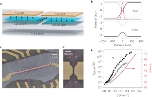
The existence of inequivalent valleys K and K′ in the momentum space of 2D hexagonal lattices provides a new electronic degree of freedom, the manipulation of which can potentially lead to new types of electronics, analogous to the role played by electron spin1,2,3. In materials with broken inversion symmetry, such as an electrically gated bilayer graphene (BLG)4,5, the momentum-space Berry curvature Ω carries opposite sign in the K and K′ valleys. A sign reversal of Ω along an internal boundary of the sheet gives rise to counterpropagating 1D conducting modes encoded with opposite-valley indices. These metallic states are topologically protected against backscattering in the absence of valley-mixing scattering, and thus can carry current ballistically1,6,7,8,9,10,11. In BLG, the reversal of Ω can occur at the domain wall of AB- and BA-stacked domains12,13,14, or at the line junction of two oppositely gated regions6. The latter approach can provide a scalable platform to implement valleytronic operations, such as valves and waveguides9,15, but it is technically challenging to realize. Here, we fabricate a dual-split-gate structure in BLG and present evidence of the predicted metallic states in electrical transport. The metallic states possess a mean free path (MFP) of up to a few hundred nanometres in the absence of a magnetic field. The application of a perpendicular magnetic field suppresses the backscattering significantly and enables a junction 400 nm in length to exhibit conductance close to the ballistic limit of 4e2/h at 8 T. Our experiment paves the way to the realization of gate-controlled ballistic valley transport and the development of valleytronic applications in atomically thin materials.
This is a preview of subscription content, access via your institution
Access options
Subscribe to this journal
Receive 12 print issues and online access
$259.00 per year
only $21.58 per issue
Buy this article
- Purchase on Springer Link
- Instant access to full article PDF
Prices may be subject to local taxes which are calculated during checkout


References
Xiao, D., Chang, M.-C. & Niu, Q. Berry phase effects on electronic properties. Rev. Mod. Phys. 82, 1959–2007 (2010).
Xu, X., Yao, W., Xiao, D. & Heinz, T. F. Spin and pseudospins in layered transition metal dichalcogenides. Nat. Phys. 10, 343–350 (2014).
Rycerz, A., Tworzydlo, J. & Beenakker, C. W. J. Valley filter and valley valve in graphene. Nat. Phys. 3, 172–175 (2007).
McCann, E. & Koshino, M. The electronic properties of bilayer graphene. Rep. Prog. Phys. 76, 056503 (2013).
Zou, K. & Zhu, J. Transport in gapped bilayer graphene: the role of potential fluctuations. Phys. Rev. B 82, 081407 (2010).
Martin, I., Blanter, Y. M. & Morpurgo, A. F. Topological confinement in bilayer graphene. Phys. Rev. Lett. 100, 036804 (2008).
Li, J., Morpurgo, A. F., Büttiker, M. & Martin, I. Marginality of bulk-edge correspondence for single-valley Hamiltonians. Phys. Rev. B 82, 245404 (2010).
Jung, J., Zhang, F., Qiao, Z. & MacDonald, A. H. Valley-Hall kink and edge states in multilayer graphene. Phys. Rev. B 84, 075418 (2011).
Qiao, Z., Jung, J., Niu, Q. & MacDonald, A. H. Electronic highways in bilayer graphene. Nano Lett. 11, 3453–3459 (2011).
Zarenia, M., Pereira, J. M. Jr, Farias, G. A. & Peeters, F. M. Chiral states in bilayer graphene: magnetic field dependence and gap opening. Phys. Rev. B 84, 125451 (2011).
Zhang, F., MacDonald, A. H. & Mele, E. J. Valley Chern numbers and boundary modes in gapped bilayer graphene. Proc. Natl Acad. Sci. USA 110, 10546–10551 (2013).
Alden, J. S. et al. Strain solitons and topological defects in bilayer graphene. Proc. Natl Acad. Sci. USA 110, 11256–11260 (2013).
Vaezi, A., Liang, Y., Ngai, D. H., Yang, L. & Kim, E.-A. Topological edge states at a tilt boundary in gated multilayer graphene. Phys. Rev. X 3, 021018 (2013).
Ju, L. et al. Topological valley transport at bilayer graphene domain walls. Nature 520, 650–655 (2015).
Qiao, Z. et al. Current partition at topological channel intersections. Phys. Rev. Lett. 112, 206601 (2014).
Yao, W., Xiao, D. & Niu, Q. Valley-dependent optoelectronics from inversion symmetry breaking. Phys. Rev. B 77, 235406 (2008).
Mak, K. F., McGill, K. L., Park, J. & McEuen, P. L. The valley Hall effect in MoS2 transistors. Science 344, 1489–1492 (2014).
Gorbachev, R. V. et al. Detecting topological currents in graphene superlattices. Science 346, 448–451 (2014).
Shimazaki, Y., Yamamato, M., Borzenets, I. V., Watanabe, K., Taniguchi, T. & Tarucha, S . Generation and detection of pure valley current by electrically induced Berry curvature in bilayer graphene. Nat. Phys. 11, 1032–1036 (2015).
Sui, M. et al. Gate-tunable topological valley transport in bilayer graphene. Nat. Phys. 11, 1027–1031 (2015).
Li, J., Martin, I., Buttiker, M. & Morpurgo, A. F. Topological origin of subgap conductance in insulating bilayer graphene. Nat. Phys. 7, 38–42 (2011).
Dean, C. R. et al. Boron nitride substrates for high-quality graphene electronics. Nat. Nanotech. 5, 722–726 (2010).
Datta, S. Electronic Transport in Mesoscopic Systems (Cambridge Univ. Press, 1997).
Engels, S. et al. Limitations to carrier mobility and phase-coherent transport in bilayer graphene. Phys. Rev. Lett. 113, 126801 (2014).
Stabile, A. A., Ferreira, A., Li, J., Peres, N. M. R. & Zhu, J. Electrically tunable resonant scattering in fluorinated bilayer graphene. Phys. Rev. B 92, 121411 (2015).
Koenig, M. et al. Quantum spin Hall insulator state in HgTe quantum wells. Science 318, 766–770 (2007).
Maciejko, J. et al. Kondo effect in the helical edge liquid of the quantum spin Hall state. Phys. Rev. Lett. 102, 256803 (2009).
Law, K. T., Seng, C. Y., Lee, P. A. & Ng, T. K. Quantum dot in a two-dimensional topological insulator: the two-channel Kondo fixed point. Phys. Rev. B 81, 041305 (2010).
Väyrynen, J. I., Goldstein, M. & Glazman, L. I. Helical edge resistance introduced by charge puddles. Phys. Rev. Lett. 110, 216402 (2013).
Väyrynen, J. I., Goldstein, M., Gefen, Y. & Glazman, L. I. Resistance of helical edges formed in a semiconductor heterostructure. Phys. Rev. B 90, 115309 (2014).
Mazio, V, Shimshoni, E, Huang, C.-W., Carr, S. T. & Fertig, H. A. Helical quantum Hall edge modes in bilayer graphene: a realization of quantum spin-ladders. Phys. Scripta T165, 014019 (2015).
Recher, P., Nilsson, J., Burkard, G. & Trauzettel, B. Bound states and magnetic field induced valley splitting in gate-tunable graphene quantum dots. Phys. Rev. B 79, 085407 (2009).
Abanin, D. A. & Levitov, L. S. Quantized transport in graphene p–n junctions in a magnetic field. Science 317, 641–643 (2007).
Zhu, J. Transport in bilayer and trilayer graphene: band gap engineering and band structure tuning. APS March Meeting http://meetings.aps.org/link/BAPS.2014.MAR.B30.1 (2014).
Garcia, A. G. F. et al. Effective cleaning of hexagonal boron nitride for graphene devices. Nano Lett. 12, 4449–4454 (2012).
Acknowledgements
J.L., Z.Z. and J.Z. are supported by the Office of Naval Research under grant no. N00014-11-1-0730 and by the National Science Foundation (NSF) grant no. DMR-1506212. K.J.M. was supported by the NSF National Nanofabrication Infrastructure Network (NNIN) Research Experience for Undergraduates Program in 2013. K. Wang, Y.R. and Z.Q. are supported by the China Government Youth 1000-Plan Talent Program, the Fundamental Research Funds for the Central Universities (grant nos WK3510000001 and WK2030020027), the National Natural Science Foundation of China (grant no. 11474265) and the National Key R&D Program (grant no. 2016YFA0301700). K. Watanabe and T.T. are supported by the Elemental Strategy Initiative conducted by MEXT, Japan, and a Grant-in-Aid for Scientific Research on Innovative Areas ‘Science of Atomic Layers’ from Japan Society for the Promotion of Science (JSPS). T.T. is also supported by a Grant-in-Aid for Scientific Research on Innovative Areas ‘Nano Informatics’ (grant no. 25106006) from JSPS. Part of this work was performed at the National High Magnetic Field Laboratory (NHMFL), which was supported by NSF through NSF-DMR-0084173 and the State of Florida. The Supercomputing Center of the University of Science and Technology of China is acknowledged for the high-performance computing assistance. The authors acknowledge the use of facilities at the Pennsylvania State University site of NSF NNIN. We are grateful for helpful discussions with R. Du, H. Fertig, D. Goldhaber-Gordon, W. Halperin, S. Ilani, J. Jain, E. Kim, C. Liu, X. Li, A. H. MacDonald, Q. Niu, A. Paramekanti and A. Young. We thank J. Jaroszynski of the NHMFL for experimental assistance.
Author information
Authors and Affiliations
Contributions
J.Z. and J.L. conceived the experiment. J.L. designed and fabricated the devices and made the measurements. K.J.M. assisted in optimizing the procedure used to fabricate the bottom split gates. J.L. and Z.Z. performed the COMSOL simulations. J.L. and J.Z. analysed the data. K. Wang, Y.R. and Z.Q. did the theoretical calculations. K. Watanabe and T.T. synthesized the h-BN crystals. J.L., J.Z., K. Wang, Y.R. and Z.Q. wrote the manuscript with input from all authors.
Corresponding authors
Ethics declarations
Competing interests
The authors declare no competing financial interests.
Supplementary information
Supplementary information
Supplementary information (PDF 2158 kb)
Rights and permissions
About this article
Cite this article
Li, J., Wang, K., McFaul, K. et al. Gate-controlled topological conducting channels in bilayer graphene. Nature Nanotech 11, 1060–1065 (2016). https://doi.org/10.1038/nnano.2016.158
Received:
Accepted:
Published:
Issue Date:
DOI: https://doi.org/10.1038/nnano.2016.158
This article is cited by
-
Dynamic topological domain walls driven by lithium intercalation in graphene
Nature Nanotechnology (2023)
-
Strain engineering of electronic properties and anomalous valley hall conductivity of transition metal dichalcogenide nanoribbons
Scientific Reports (2022)
-
Interplay between topological valley and quantum Hall edge transport
Nature Communications (2022)
-
Robust all-electrical topological valley filtering using monolayer 2D-Xenes
npj 2D Materials and Applications (2022)
-
Recent progresses of quantum confinement in graphene quantum dots
Frontiers of Physics (2022)


