Collection 

Special Issue on Nanostructures in Photonics

More than six decades passed, since the first patent and publications on the importance of quantum wells (QWs), two-dimensional nano-heterostructures, for reducing the threshold current density and thus increasing the efficiency and output power of semiconductor lasers by Dingle and Henry. Breakthroughs of heterostructure growth based on the development of MBE (molecular beam epitaxy) and MOCVD (metal-organic chemical vapor deposition) presented the basis of this progress. Today one can praise QW-lasers as the first “green” lasers.  Close to 100% of all semiconductor lasers using all kinds of material systems are now based on quantum wells. Theoretical work predicted that, reducing further the dimensionality of the gain material to 1D and 0D structures, should additionally lead to huge advantages of performance of lasers. Smaller threshold current densities, larger material gain, larger modulation frequency, increased temperature stability were dreamed of.  Attempts to extend the quantum well success story to quantum wires and “technology based” quantum dots, where quantum well laser structures were etched to create nano-size pillars, failed to produce superior devices operating again at room temperature like QW-lasers.

The discovery of self-organized growth in strained hetero-structures (Stranski-Krastanov, submonolayer deposition,..) in the 1990s, to create large densities of quantum dots, showing actually more than the predicted huge material gain, lead to an explosion of research on nanostructures and their applications for a large diversity of devices all around the world. As of today, Google Scholar counts ~ 3 million of publications on this subject. QD-lasers show today the lowest threshold current density of 6 A/cm2 per QD-layer, the best temperature stability,… of all semiconductor lasers. Passively mode-locked lasers generate hat-like frequency combs enabling bit rates in the 4-5 Tb/s range. Quantum dots  conquered in the last years territory not thought about 30 years ago, like becoming simple to fabricate sources for q-bit and entangled photon emitters, probably soon operating at room temperature, for novel memories combining the best of flash and DRAM, hailed as the “holy grail of memories”.

This volume provides the readers with a glimpse to a variety of most recent and important achievements on some of the most important areas of research on such nanostructures.


Special Issue on Nanostructures in Photonics

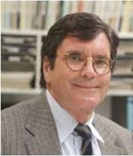
Guest Editor: Prof. Dr. Dr. h. c. mult. Dieter Bimberg

Prof. Dieter Bimberg is the founding director of the Center of NanoPhotonics at Technical University of Berlin, and now the executive director of the Bimberg Chinese-German Center for Green Photonics of the Chinese Academy of Sciences at CIOMP, Changchun, China. He is Member of the German Academy of Sciences, Foreign Member of the National Academy of Engineering and of the National Academy of Inventors of the USA, and Member of the Russian Academy of Sciences. He is presently Vice-Chair and incoming Chair (2023-2024) of the Electronics, Communication and Informations Systems Engineering Search Committee of the National Academy of Engineering of the USA.

He pioneered together with his students the general effective mass, 8-band k.p and many particle theories of quantum dots, presenting the basis to understand the electronic, optical, and transport properties of QDs and QD devices. His fundamental discovery of the relevance of strain for self-organized growth established novel growth technologies for devices with properties superior to those of quantum-well structures. Together with the MBE team of the Nobel Laureate Z. I. Alferov the first low- and room-temperature injection lasers based on self-organized quantum dots were demonstrated. Briefly later his Berlin team achieved the world record of lowest threshold current density for any semiconductor lasers, using MOCVD of QDs, being the mass production tool for photonic devices. He introduced QDs as active areas in ultra-high speed mode-locked lasers, semiconductor optical amplifiers, high speed single photon emitters and novel quantum dot based memories, combining the best of DRAM and Flash. Most recently his work focusses on the energy-efficiency of photonic devices, edge and surface emitting lasers for a multitude of wavelengths, and systems based there upon.

He is a living legend of nanostructures and semiconductor devices and the initiator and brain of many scientific cooperations around the globe. This special volume on "Nanostructures in Photonics" is presenting invited work of some of the most important present contributors of his field, illuminating their important recent achievements.